In our previous post, I explained the GPIO and the external interrupt. Now let’s move the new chapter, the ADC(Analog to Digital Converter) in polling method. If you want to explore the ADC interrupt method, please have a look here.
Some basics about ADC
An ADC in a microcontroller is a component that converts analog signals (continuous signals) into digital signals (binary values) that the microcontroller or any other digital circuits can process. The ADC’s resolution, expressed in bits, determines the number of discrete values it can produce, with higher resolution offering finer granularity.
The sampling rate, or frequency at which the ADC samples the analog input, impacts how accurately the signal is captured. The voltage reference (Vref) defines the maximum voltage the ADC can convert, setting the upper limit of the analog input range. Microcontrollers often feature multi-channel ADCs, allowing multiple analog inputs to be sampled.
ADC in STM32F103C6T6A
In STM32F103C6T6A has two ADCs with 12 bit resolution – ADC1 and ADC2 (Refer Table 2 of the datasheet). In the reference manual section 11.3.3 says the microcontroller has 16+1 ADC channels. This is the number of channels supported by the ADC module used in our microcontroller. But if you check the datasheet, there are only 10 ADC12_INx pins available. Check the table shown in the pinout and pin description section.
Regular and Injected group: It is possible to use the ADC as two different groups namely Regular Group and Injected Group. The regular group can have maximum 16 conversions. This group is used for periodic measurements such as monitoring sensor values, where the exact timing of each measurement is not critical. Where as the injected group is used for more urgent measurements that need to be taken at specific times or in response to specific events, like sudden changes in a system’s state that require immediate attention. The injected conversions have higher priority over regular conversions, allowing them to interrupt and take precedence.
Modes of operations: The ADC can work in four modes
- Single conversion mode — The ADC does the conversion upon setting the ADON bit set (Regular conversions) or by external trigger (Regular and injected conversion) and the CONT bit should set as 0.
- Continuous conversion mode — The continuous mode will start another conversion as soon as the current conversion is finished.
- Scan Mode — This mode allows conversion of multiple channels in a specified sequence. It can be used with either single conversion mode (converting all channels once) or continuous conversion mode (converting all channels repeatedly).
- Discontinuous mode — This mode converts a specified number of channels in the sequence, then pauses allowing CPU to do the data processing or other tasks between conversion groups.
In all the modes explained above, except Single Conversion mode, for each conversion the data will be written into the ADC_DR register. However, there is a high chance of missing some data if we are using the polling or interrupt method. The best approach to work with Continuous mode is DMA.
Exercise
As we did in the other post, let’s try to understand the working of ADC using an exercise. Here is your task. You can refer the dev setup of STM32 bluepill here
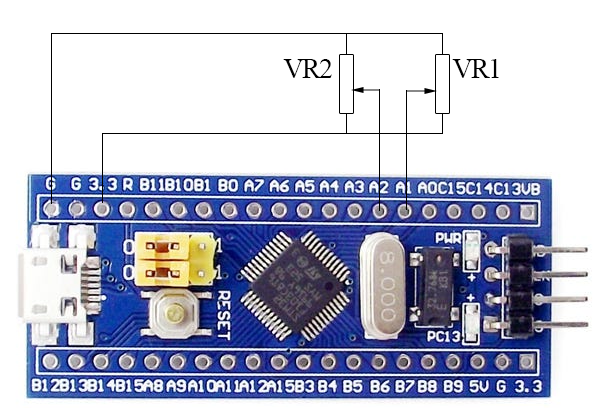
Write an LED blinking program using two ADC channels, where the first channel should control the ON duration of LED (duty cycle) and second channel should control the frequency of blinking. You can use any potentiometre or preset for giving different voltage to the input channels as shown below.
Registers used
The following registers are used to solve the tasks
- APB2 peripheral clock enable register (RCC_APB2ENR) – Enable clock for ADC and GPIO port A and C
- Port configuration register high for port C (GPIOC_CRH) – Enable GPIO port C output for built-in LED
- Port configuration register high for port A (GPIOA_CRL) – Enable the analog input channels
- ADC Control Register 2 (ADC_CR2) – ADC enable and calibration.
- ADC Regular Sequence Register 3 (ADC_SQR3) – Specify the channels to be converted
- ADC Status Register (ADC_SR) – Check if the conversion completed or not
- ADC Data Register (ADC_DR) – Get the converted data.
Solution
Before proceeding to the solution, I strongly recommend thoroughly reviewing the ADC section of the reference manual to gain a basic understanding of the ADC. The main focus should be on the bit fields in the registers mentioned above.
As usual, first we need to enable for the peripherals. In this case we have to blink the LED (GPIO-PORTC) taking the input from the analog pins (GPIO-PORTA). We have two ADC in this microcontroller, I am taking ADC1.
// Enable clock for GPIOA, GPIOC & ADC1 peripheral
RCC->APB2ENR |= RCC_APB2ENR_IOPCEN;
RCC->APB2ENR |= RCC_APB2ENR_IOPAEN;
RCC->APB2ENR |= RCC_APB2ENR_ADC1EN;
Now we have to configure the GPIO modes. The LED is connected to the PC13 pin, so this pin should be digital output. I am taking the ADC input channels 1 and 2 (0 based index) via PA1 and PA2 respectively.
// Configure built in LED as output
GPIOC->CRH &= ~(GPIO_CRH_CNF13 | GPIO_CRH_MODE13);
GPIOC->CRH |= GPIO_CRH_MODE13_0;

// GPIOA1 and GPIOA2  - analog input mode
GPIOA->CRL &= ~(GPIO_CRL_CNF1 | GPIO_CRL_MODE1);
GPIOA->CRL &= ~(GPIO_CRL_CNF2 | GPIO_CRL_MODE2);
The ADC can be powered-on by setting the ADON bit in the ADC_CR2 register. When the ADON bit is set for the first time, it wakes up the ADC from Power Down mode. Conversion starts when ADON bit is set for a second time by software after ADC power-up time (giving ~100ms).
ADC1->CR2 |= ADC_CR2_ADON;
delay(100);
ADC1->CR2 |= ADC_CR2_ADON;
Calibrating the ADC is the best practice and this should be done immediately after the ADC is enabled. The ADC has an built-in self calibration mode. Calibration significantly reduces accuracy errors due to internal capacitor bank variations.
ADC1->CR2 |= ADC_CR2_CAL;
while(ADC1->CR2 & ADC_CR2_CAL);
Now that the ADC setup is complete, we need to start the conversion. First, we will set the desired channel number (here, channel 1) in the first regular conversion sequence (SQ1, i.e., ADC_SQR3[4:0]). Then, we enable the ADC again by setting the ADON bit of the ADC_CR2 register once again. The conversion will start the moment this bit is set, and the EOC flag in ADC_SR will be set once the conversion is completed. The converted value would be stored in the ADC_DR register.
// Get ADC value from channel 1
ADC1->SQR3 = 1;                     // Select channel
ADC1->CR2 |= ADC_CR2_ADON;          // Enable ADC
while(!(ADC1->SR & ADC_SR_EOC));    // Wait until the End Of Conversion flag is set
adcDelay1 = ADC1->DR;               // Get the data from ADC Data Register
Similarly take the data from channel 2.
// Get ADC value from channel 2
ADC1->SQR3 = 2;
ADC1->CR2 |= ADC_CR2_ADON;
while(!(ADC1->SR & ADC_SR_EOC));
adcDelay2 = ADC1->DR;
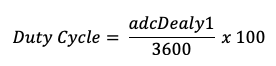
I am taking the adcDelay1 to determine the ON duration. When I print this value using UART (we will discuss how to do this in our upcoming posts), I observed that the maximum value close to 3600. Take this value as total time period. So the duty cycle can be calculated for any ADC value using the following equation.
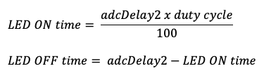
The adcDelay2 is taking as time period, also we already calculated the duty cycle in %. Now let’s calculate the ON time and OFF time
dutyCycle = adcDelay1 * 100 / 3600;

// Work-around to keep dutycycle not more than 100%
// Because in some case, the adcDelay1 is going more
// than 3600.
if(dutyCycle > 100) {
    dutyCycle = 100;
}

// Calculate the LED on and off time
onTime = (adcDelay2 * dutyCycle) / 100;
offTime = adcDelay2 - onTime;
Now let’s combine all together.
int main(void)
{
    uint16_t adcDelay1 = 0xFFF;
    uint16_t adcDelay2 = 0xFFF;

    uint16_t onTime = 0;
    uint16_t offTime = 0;
    uint8_t dutyCycle = 0;

    // Enable clock for GPIOA, GPIOC & ADC1 peripheral
    RCC->APB2ENR |= RCC_APB2ENR_IOPCEN;
    RCC->APB2ENR |= RCC_APB2ENR_IOPAEN;
    RCC->APB2ENR |= RCC_APB2ENR_ADC1EN;

    // Configure built in LED as output
    GPIOC->CRH &= ~(GPIO_CRH_CNF13 | GPIO_CRH_MODE13);
    GPIOC->CRH |= GPIO_CRH_MODE13_0;

    // GPIOA1 analog input mode
    GPIOA->CRL &= ~(GPIO_CRL_CNF1 | GPIO_CRL_MODE1);
    GPIOA->CRL &= ~(GPIO_CRL_CNF2 | GPIO_CRL_MODE2);

    // Document RM0008 Section 11.3.1
    // The ADC can be powered-on by setting the ADON bit in the
    // ADC_CR2 register. When the ADON bit is set for the first
    // time, it wakes up the ADC from Power Down mode. Conversion
    // starts when ADON bit is set for a second time by software
    // after ADC power-up time (giving ~100ms)
    ADC1->CR2 |= ADC_CR2_ADON;
    delay(100);
    ADC1->CR2 |= ADC_CR2_ADON;

    // Caliberate ADC after each power up
    ADC1->CR2 |= ADC_CR2_CAL;
    while(ADC1->CR2 & ADC_CR2_CAL);

    // Turn LED off
    TOGGLE_LED();

    while (1) {
        // Get ADC value from channel 1
        ADC1->SQR3 = 1;                     // Select channel
        ADC1->CR2 |= ADC_CR2_ADON;          // Enable ADC
        while(!(ADC1->SR & ADC_SR_EOC));    // Wait until the End Of Conversion flag is set
        adcDelay1 = ADC1->DR;               // Get the data from ADC Data Register

        // Get ADC value from channel 2
        ADC1->SQR3 = 2;
        ADC1->CR2 |= ADC_CR2_ADON;
        while(!(ADC1->SR & ADC_SR_EOC));
        adcDelay2 = ADC1->DR;

        dutyCycle = adcDelay1 * 100 / 3600;

        // Work-around to keep dutycycle not more than 100%
        // Because in some case, the adcDelay1 is going more
        // than 3600.
        if(dutyCycle > 100) {
            dutyCycle = 100;
        }

        // Calculate the LED on and off time
        onTime = (adcDelay2 * dutyCycle) / 100;
        offTime = adcDelay2 - onTime;

        // Toggle
        TOGGLE_LED();
        delay(onTime);
        TOGGLE_LED();
        delay(offTime);
    }
}
Please find the complete source code in my github repository.
Here is the video of my attempt.
Pingback: STM32F103 ADC Interrupt method - Register-level Programming
Pingback: STM32F103C6T6A ADC with DMA – Bare Metal Programming Guide