In our previous blog post, we dove into the intricate workings of the Universal Serial Interface (USI) transmitting data via UART. Now, we shift our focus to the other half of the conversation: receiving data. This time, we’ll skip the protocol-level explanations since we’ve covered them extensively in our previous discussions: Mastering UART – A comprehensive overview. Instead, we’ll jump right into the practical aspect of utilizing the USI for UART data reception. We’ll explore how to implement the USI as a receiver in real-world scenarios, equipping you with the knowledge to integrate this functionality seamlessly into your projects. So, if you’re ready to explore the realm of UART data reception with the USI, let’s get started.
In this blog, we’ll construct a UART receiver circuit featuring an LED. This circuit will have the ability to receive an integer input, with the LED blinking a number of times corresponding to the value received through the UART, ranging from 0 to 255.
USI Initialization as UART

In the provided circuit diagram, our focus lies on the components highlighted in green, as these are essential for integrating the UART module described earlier.
Here I am using the USI module in 3 pin communication mode and clock source as Timer/Counter0 compare match. So the data input pin will be DI (PB0).
Start with USI disabled and enable the pin change interrupt on PB0 (PCINT0).
static void setup_usi_uart_rx() {
    DDRB &= ~(1 << DATA_IN_PIN);    // Set DI pin as input
    PORTB |= (1 << DATA_IN_PIN);    // Set the output high in idle
    USICR = 0;                      // Start with USI disabled
    GIMSK |= (1 << PCIE);           // Enable pin change interrupt
    PCMSK |= (1 << PCINT0);         // Enable interrupt for PB0
    sei();                          // Enable global interrupt
}
Implement the ISR for data receive
The idle state of the communication link is logically high. Any data packet coming through the line will start with a start bit logic low. So, wait until a high-to-low transition occurs on pin PB0. Whenever PB0 receives the pin change interrupt (PCINT0), disable PCINT0.
ISR(PCINT0_vect) {
    // start_timer1();
    if(0 == (PINB & (1 << PB0))) {
        GIMSK &= ~(1 << PCIE);        // Disable the pin change interrupt
        on_uart_data_rx();
    }
}
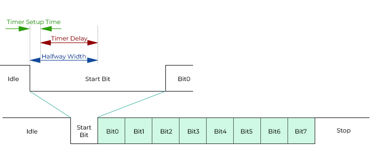
Configure Timer/Counter0 in Compare mode to reach halfway through the start bit. This is essential to reduce data reception errors. Refer the following diagram

void on_uart_data_rx() {
    TCCR0A |= (1 << WGM01);                 // Clear timer on compare match
    GTCCR  |= (1 << PSR0);                  // Reset prescaler
    OCR0A = HALF_BIT_WIDTH - START_BIT_FIX; // Set the counter value
    TCNT0 = 0;                              // Start counting from 0
    TIFR |= (1 << OCF0A);         // Clear Timer0 compare match interrupt flag
    TIMSK |= (1 << OCIE0A);       // Enable Timer0 compare match interrupt
    TCCR0B |= (1 << CS01);        // Set prescaler 8 to clk
}
Determine the compare value while taking into account the CPU cycle required for configuring Timer/Counter0 in compare mode and setting up the USI counter overflow interrupt. The constant START_BIT_FIX, calculated as 53 divided by the prescaler, is utilized for this purpose. The value 53 is calculated with the help of the timing of Timer/Counter1. To obtain this value, Timer/Counter1 is initiated immediately after the PCINT0 interrupt and halted once the prescaler is configured. Subsequently, the observed value of TCNT1 was 53.
Wait until the halfway of start bit is reached. Configure the USI and USI Counter overflow interrupt with initial counter value as 8 so that we will get the interrupt when 1 byte of data is received.
Implement ISR for data complete
ISR(TIMER0_COMPA_vect) {
    TIMSK &= ~(1 << OCIE0A);       // Enable Timer0 compare match interrupt
    TCNT0 = 0;
    OCR0A = FULL_BIT_WIDTH;
    USICR |= (1 << USIOIE) |                    // Enabled overflow interrupt
             (0 << USIWM1) | (1 << USIWM0) |    // Enable 3 wire mode - data input to PB0
             (0 << USICS1) | (1 << USICS0) | (0 << USICLK);  // Select Timer0 Compare match

    USISR |= (1 << USIOIF) | 8;                 // Clear overflow interrupt flag
}
Wait until the USI Counter overflow interrupt is triggered and copy the data from USIBR to appropriate variable and re-enabled the PCINT0. Stop the USI and wait for the next start bit
ISR (USI_OVF_vect) {
    data_buff = USIBR;
    USICR = 0;
    GIFR |= (1 << PCIF);                    // Clear pin change interrupt flag
    GIMSK |= (1 << PCIE);                   // Enable pin change interrupt
}
Here is the complete source code in my Github page
Pingback: Understanding I2C Protocol: Fundamentals & Applications