One of the important feature of STM32F103C6T6A is the DMA. This feature significantly optimizes data handling and processing efficiency. In this blog post, we will explore the capabilities of the DMA controller and demonstrate its practical application using the Analog-to-Digital Converter (ADC). We already have covered ADC in polling and interrupt methods. If you are an ADC beginner, I recommend to check those post before proceeding this blog post.
What is DMA?
Direct Memory Access (DMA) allows peripherals to transfer data directly to and from memory without requiring constant CPU intervention. This functionality is particularly beneficial in applications where continuous data flow and real-time processing are crucial. By offloading data transfer tasks to the DMA controller, the CPU can perform other operations or enter low-power modes, thereby improving overall system efficiency.
ADC with DMA
I have already written a couple of blogs related to using the ADC, covering both the polling and interrupt methods. However, those approaches are useful primarily when a single channel is used for ADC. When multiple channels are involved, the converted data may be overwritten since the register where the result is stored is the same. This is where DMA comes into play. When combined with DMA, the ADC can continuously sample and transfer conversion results to memory autonomously. This setup is ideal for scenarios where high-speed, real-time data acquisition is needed from multiple ADC channels without burdening the CPU with repetitive tasks.
Exercise
Write a program to read voltage from three different channels and blink an LED based on the data received from each channel. The ON/OFF delay should be equivalent to the milliseconds of the converted data from each channel.
For example: If the converted data are 1000, 500, and 3000, then the LED should first turn on and then off for 1000ms, then turn on and off for 500ms, and then turn on and off for 3000ms. This should continue in a loop.
Solution
Pin Selection
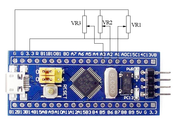
STM32F103C6T6A has two ADC module with 10 channel each (But only 7 channels are exposed in the board). But both set of channels are sharing the same set of pins. The ‘table 5: pinout and pin description’ in the datasheet shows the pin associated with each channels. As per the requirement we need 3 channels, so I am taking the channel 1, 2 and 3 of the ADC1 (Please not that the channel number start from 0).
So the circuit diagram would be like this
Registers to be used
- APB2 peripheral clock enable register (RCC_APB2ENR) –
- Port configuration register low (GPIOA_CRL) –
- Port configuration register high (GPIOC_CRH) –
- ADC control register 1 (ADC_CR1) –
- ADC control register 2 (ADC_CR2) –
- ADC regular sequence register 1 (ADC1_SQR1) –
- ADC regular sequence register 3 (ADC1_SQR3) –
- AHB peripheral clock enable register (RCC_AHBENR) –
- DMA channel 1 configuration register (DMA_CCR1 or DMA1_Channel1_CCR) –
- DMA channel 1 number of data register (DMA_CNDTR1 or DMA1_Channel1_CNDTR) –
- DMA channel 1 peripheral address register (DMA_CPAR1 or DMA1_Channel1_CPAR) –
- DMA channel 1 memory address register (CMA_CMAR1 or DMA1_Channel1_CMAR) –
Source code implementation
Initially we need to setup the ADC. You can refer my previous posts, datasheet, reference manual and try to create your own ADC setup code. The ADC should be configured in the scan mode with three channels as mentioned above and enable the DMA for the ADC. Here is my ADC setup code
// Enable clock for GPIOA & ADC1 peripheral
RCC->APB2ENR |= RCC_APB2ENR_IOPAEN;                     // Analog input
RCC->APB2ENR |= RCC_APB2ENR_ADC1EN;                     // ADC peripheral

// GPIOA1, GPIOA2 and GPIOA3 as analog input mode
GPIOA->CRL &= ~(GPIO_CRL_CNF1 | GPIO_CRL_MODE1);
GPIOA->CRL &= ~(GPIO_CRL_CNF2 | GPIO_CRL_MODE2);
GPIOA->CRL &= ~(GPIO_CRL_CNF3 | GPIO_CRL_MODE3);

ADC1->CR1 |= ADC_CR1_SCAN;                              // Enable scan mode

ADC1->CR2 |= ( ADC_CR2_CONT   |                         // Continuous mode
               ADC_CR2_DMA    |                         // Enable DMA
               // Right align by default
               ADC_CR2_EXTSEL |                         // Start conversion by setting SWSTART bit
               ADC_CR2_EXTTRIG );                       // Start conversion on external trigger

ADC1->SQR1 |= (2 << ADC_SQR1_L_Pos);                    // 2 for 3 channels

ADC1->SQR3 = ( (ADC_SQR3_SQ1_0) |                       // 1st conversion - channel 1
               (ADC_SQR3_SQ2_1) |                       // 2nd conversion - channel 2
               (ADC_SQR3_SQ3_0 | ADC_SQR3_SQ3_1) );     // 3rd Conversion - channel 3

// Document RM0008 Section 11.3.1
// The ADC can be powered-on by setting the ADON bit in the
// ADC_CR2 register. When the ADON bit is set for the first
// time, it wakes up the ADC from Power Down mode. Conversion
// starts when ADON bit is set for a second time by software
// after ADC power-up time
ADC1->CR2 |= ADC_CR2_ADON;
delay(100);

// Calibrate ADC after each power up
ADC1->CR2 |= ADC_CR2_CAL;
while(ADC1->CR2 & ADC_CR2_CAL);
Next step is setup the DMA. As usual enable the clock for the DMA controller
// Enable clock for DMA
RCC->AHBENR |= RCC_AHBENR_DMA1EN;
We have already setup the ADC. When the ADC is started the converted data would be stored in the ADC_DR register. We have to copy this data (from peripheral) to a variable (memory). So the DMA data direction is from peripheral to memory.
DMA1_Channel1->CCR &= ~(DMA_CCR_DIR);
Even though the ADC resolution is 10bit, the register used for storing the data is 16 bit. So the peripheral data and memory data size are 16 bit. Also, the source location is constant and we need to write the data in destination in circular manner.
DMA1_Channel1->CCR |= (DMA_CCR_CIRC    |               // Enable ciruclar buffer
                       // DMA_CCR_PINC |               // Peripheral address is always constant
                       DMA_CCR_MINC    |               // Enable memory address increment
                       DMA_CCR_PSIZE_0 |               // Peripheral data size 16 bit
                       DMA_CCR_MSIZE_0 );              // Memory data size 16 bit
Now set the data size, we have 3 ADC, so data size is 3. Configure peripheral and memory starting addresses and finally enable the DMA. The memory address can be a variable array of 16 bit integers of size 3.
DMA1_Channel1->CNDTR = 3;                              // Data size 3 (3 ADC channels)
DMA1_Channel1->CPAR = (uint32_t)&ADC1->DR;
DMA1_Channel1->CMAR = (uint32_t)adc_data_buff;
DMA1_Channel1->CCR |= DMA_CCR_EN;
We have started the ADC and DMA. So the data from ADC output register will be copied array of integer. This data can be used to blink the LED.
Here is the complete source code