In the previous post, I showed how to build STM32 code on Ubuntu. I also explained how to flash it to the STM32F103C6T6A board.
Now, let’s focus on GPIO. This guide will show you how to use GPIO pins as input and output. We’ll cover different modes and configurations.
You’ll need the datasheet and reference manual. I shared both in the last post.
For GPIO, check Section 9 of the reference manual. Table 2 in the datasheet says this chip has 37 GPIO pins.
To understand the ports and pin count, let’s look at the pinout diagram.
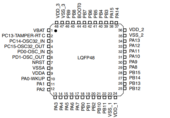
From the pinout, it’s clear that we have PortA (PA0-PA15), PortB (PB0-PB15), PortC (PC13-PC15) and PortD (PD0-PD1) so total 37 pins.
For configuring the pin, we have to configure the following registers. The letter “x” represents the name of the port, which can be A, B, C, or D based on the selected port.
- APB2 Peripheral Reset Register (RCC_APB2RSTR) – Used to enable clock to the GPIO peripheral
- Port Configuration Register Low (GPIOx_CRL) – Configure the GPIO pin from 0 to 7
- Port Configuration Register High (GPIOx_CRH) – Configure the GPIO pin from 8 to 15
- Port Input Data Register (GPIOx_IDR) – Used only when pin is configured as input
- Port Output Data Register (GPIOx_ODR) – Configure the output data (0 or 1) when the pin is configured as output and pull-up/pull-down when pin is configured as input
- Port Bit Set/Reset Register (GPIOx_BSRR) – Same usage as GPIOx_ODR but atomic bit set/reset allowed
- Port Bit Reset Register (GPIOx_BRR) – Reset the GPIOx_ODR bits
- Port Configuration Lock Register (GPIOx_LCKR) – Freeze the corresponding 4 bits in the GPIOx_CRL/CRH
Please refer section 9.2 of the reference manual for more details about each bits in the above registers.
Exercise
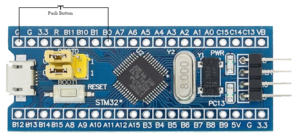
In the development board of STM32F103C6T6, there is built in LED connected in PC13. Connect a switch to PB0 as shown in the diagram below. Write a program to blink LED 3 times when the button is pressed and then released.
Download the empty project and start from here.
How to configure registers
In this project, all register addresses are mapped with corresponding names. Moreover, for each register, structures are defined to configure each registers easily. These definitions and mappings are done in the Drivers/CMSIS/Device/ST/STM32F1xx/Include/stm32f103x6.h file.
For example there are several registers associated with reset and clock control like RCC_CR, RCC_CFGR, RCC_CIR, etc. All the registers are encapsulated in to a single C structure in the following way.
typedef struct {
    __IO uint32_t CR;
    __IO uint32_t CFGR;
    __IO uint32_t CIR;
    __IO uint32_t APB2RSTR;
    __IO uint32_t APB1RSTR;
    __IO uint32_t AHBENR;
    __IO uint32_t APB2ENR;
    __IO uint32_t APB1ENR;
    __IO uint32_t BDCR;
    __IO uint32_t CSR;
} RCC_TypeDef;

#define PERIPH_BASE           0x40000000UL
#define AHBPERIPH_BASE        (PERIPH_BASE + 0x00020000UL)
#define RCC_BASE              (AHBPERIPH_BASE + 0x00001000UL)
#define RCC                   ((RCC_TypeDef *)RCC_BASE)
We can access or configure the data in these registers by accessing the members of the structure. To enable the clock to GPIO port C, we have to set the IOPCEN bit of the APB2ENR register. This can be achieved by using the following code.
RCC->APB2ENR |= RCC_APB2ENR_IOPCEN;
RCC_APB2ENR_IOPCEN is defined in the same header file.
Solution
We are using the GPIO pins from port B and port C. Enable the clock for GPIOB and GPIOC as explained above. The section and table I have referred to in this post is from the STM32 reference manual.
// Enable clock for GPIOC and GPIOB peripherals
RCC->APB2ENR |= (RCC_APB2ENR_IOPCEN | RCC_APB2ENR_IOPBEN);
Now configure the GPIO pin. We have to configure the PB0 as input and PC13 as output.
To configure PB0 as input, use the GPIOx_CRL register. This is explained in section 9.2.1 of the STM32 reference manual.
Set MODE0 to 00 for input mode. Set CNF0 to 10 for input with pull-up or pull-down.
In our setup, the switch connects to ground. When pressed, PB0 reads as 0.
Since there’s no external power, we need a pull-up. This keeps the pin high when the switch is not pressed.
Enable the internal pull-up by setting the ODR0 bit in the GPIOB_ODR register.
You’ll find more on this in Table 20 of the reference manual.
// Configure PB0 pin as input pull up or pull down
GPIOB->CRL &= ~(GPIO_CRL_CNF0 | GPIO_CRL_MODE0);
GPIOB->CRL |= GPIO_CRL_CNF0_1;

// PBO as pull up
GPIOB->ODR |= GPIO_ODR_ODR0;
For configuring PC13, which is after the first 8 bits, we can use GPIOx_CRH (referenced in section 9.2.2 of the reference manual). Configure MODE13 as 01 (Output mode maximum speed 10MHz) and CNF13 as 00 (General-purpose output push-pull). For more information about push-pull configuration, read this post.
// Configure GPIO pin as output push-pull maximum speed 10MHz
GPIOC->CRH &= ~(GPIO_CRH_CNF13 | GPIO_CRH_MODE13);
GPIOC->CRH |= GPIO_CRH_MODE13_0;
So the GPIO pins are set up now. In the reset condition, the GPIO pin will be up. Turn it off by writing 1 to the GPIOC_ODR register.
// By default the output pin will be high, turn it off
GPIOC->ODR |= GPIO_ODR_ODR13;
I have created the following function and defined some macros to enable enable and disable the built in LED.
#define TURN_ON_LED()            turn_led_on(TURN_ON)
#define TURN_OFF_LED()           turn_led_on(TURN_OFF)
#define TOGGLE_LED()             turn_led_on(TURN_TOGGLE)

typedef enum {
    TURN_OFF,
    TURN_ON,
    TURN_TOGGLE
} LedState_t;

void turn_led_on(LedState_t state) {
    if(state == TURN_TOGGLE){
        GPIOC->ODR ^= GPIO_ODR_ODR13;
    } else if(state == TURN_ON) {
        GPIOC->ODR &= ~(GPIO_ODR_ODR13);
    } else {
        GPIOC->ODR |= GPIO_ODR_ODR13;
    }
}
Combining all together, here the complete code
/**
  ******************************************************************************
  * @file           : main.c
  * @brief          : Main program body
  ******************************************************************************
  */
#include "main.h"

#define TURN_ON_LED()            turn_led_on(TURN_ON)
#define TURN_OFF_LED()           turn_led_on(TURN_OFF)
#define TOGGLE_LED()             turn_led_on(TURN_TOGGLE)


typedef enum {
    TURN_OFF,
    TURN_ON,
    TURN_TOGGLE
} LedState_t;

void delay(uint32_t ms) {
    // Simple delay function (not accurate, just for demonstration)
    for (volatile uint32_t i = 0; i < ms * 1000; ++i) {
        __NOP();  // No operation (compiler barrier)
    }
}

void turn_led_on(LedState_t state) {
    if(state == TURN_TOGGLE){
        GPIOC->ODR ^= GPIO_ODR_ODR13;
    } else if(state == TURN_ON) {
        GPIOC->ODR &= ~(GPIO_ODR_ODR13);
    } else {
        GPIOC->ODR |= GPIO_ODR_ODR13;
    }
}

/**
  * @brief  The application entry point.
  * @retval
  */
int main(void)
{
    uint8_t i;
    const uint8_t repeat = 3;

    // Enable clock for GPIOC and GPIOB peripherals
    RCC->APB2ENR |= (RCC_APB2ENR_IOPCEN | RCC_APB2ENR_IOPBEN);

    // Configure PC13 pin as output push-pull maximum speed 10MHz
    GPIOC->CRH &= ~(GPIO_CRH_CNF13 | GPIO_CRH_MODE13);
    GPIOC->CRH |= GPIO_CRH_MODE13_0;

    // Configure PB0 pin as input pull up or pull down
    GPIOB->CRL &= ~(GPIO_CRL_CNF0 | GPIO_CRL_MODE0);
    GPIOB->CRL |= GPIO_CRL_CNF0_1;

    // PBO as pull up
    GPIOB->ODR |= GPIO_ODR_ODR0;

    // By default the output will be high, turn it off
    TURN_OFF_LED();

    while (1) {
        // Switch is released by default. On pressing switch
        // the input will become 0 and exit the loop.
        while(GPIOB->IDR & GPIO_IDR_IDR0) {}

        // Wait here as long as switch kept as pressed
        while(!(GPIOB->IDR & GPIO_IDR_IDR0)) {}

        // Blink LED `repeat` times
        for(i = 0; i < repeat; i++) {
            TURN_ON_LED();
            delay(500);
            TURN_OFF_LED();
            delay(500);
        }
    }
    // Should not reach here.
    return 0;
}
Github link to the complete source code.
Here is the video of my attempt.
Pingback: STM32F103 EXTI Interrupt Guide | Bare-Metal Code